Loading [MathJax]/extensions/MathMenu.js
Dynamic voltage and frequency management for a low-power embedded microprocessor | IEEE Journals & Magazine | IEEE Xplore

Dynamic voltage and frequency management for a low-power embedded microprocessor


Abstract:

High-performance and low-power microprocessors are key to PDA applications. A dynamic voltage and frequency management (DVFM) scheme with leakage power compensation effec...Show More

Abstract:

High-performance and low-power microprocessors are key to PDA applications. A dynamic voltage and frequency management (DVFM) scheme with leakage power compensation effect is introduced in a microprocessor with 128-bit wideband 64-Mb embedded DRAM. The DVFM scheme autonomously controls clock frequency from 8 to 123 MHz in steps of 0.5 MHz and also adaptively controls supply voltage from 0.9 to 1.6 V in steps of 5 mV, achieving 82% power reduction in personal information management scheduler application and 40% power reduction in MPEG4 movie playback. This low-power embedded microprocessor, fabricated with 0.18-/spl mu/m CMOS embedded DRAM technology, enables high-performance operations such as audio and video applications. As process technology shrinks, this adaptive leakage power compensation scheme will become more important in realizing high-performance and low-power mobile consumer applications.
Published in: IEEE Journal of Solid-State Circuits ( Volume: 40, Issue: 1, January 2005)
Page(s): 28 - 35
Date of Publication: 31 January 2005

ISSN Information:

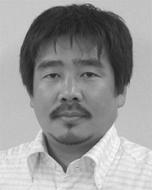
Author image of M. Nakai
Semiconductor Solutions Network Company, Sony Corporation, Tokyo, Japan
Masakatsu Nakai received the B.S. and M.S. degrees in electronics engineering from Tokai University, Tokyo, Japan, in 1988 and 1990, respectively.
In 1990, he joined Sony Corporation, Tokyo, Japan, where he developed single chip microcontrollers, memories, and analog circuits. Since 1999, he has been engaged in research and development of low-power circuits and techniques for CMOS LSI.
Masakatsu Nakai received the B.S. and M.S. degrees in electronics engineering from Tokai University, Tokyo, Japan, in 1988 and 1990, respectively.
In 1990, he joined Sony Corporation, Tokyo, Japan, where he developed single chip microcontrollers, memories, and analog circuits. Since 1999, he has been engaged in research and development of low-power circuits and techniques for CMOS LSI.View more
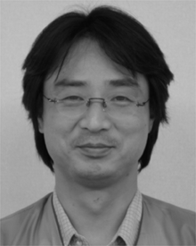
Author image of S. Akui
Semiconductor Solutions Network Company, Sony Corporation, Tokyo, Japan
Satoshi Akui received the B.S. and M.S degrees from the Tokyo Institute of Technology, Tokyo, Japan, in 1986 and 1988, respectively.
He joined Sony Corporation, Tokyo, Japan, in 1988. Since then, he has been engaged in research and development of new design methodologies. Since 2000, he has been engaged in research and development of mobile application processors.
Satoshi Akui received the B.S. and M.S degrees from the Tokyo Institute of Technology, Tokyo, Japan, in 1986 and 1988, respectively.
He joined Sony Corporation, Tokyo, Japan, in 1988. Since then, he has been engaged in research and development of new design methodologies. Since 2000, he has been engaged in research and development of mobile application processors.View more
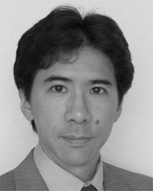
Author image of K. Seno
Semiconductor Solutions Network Company, Sony Corporation, Tokyo, Japan
Katsunori Seno received the B.S. and M.S. degrees in electrical engineering from Waseda University, Tokyo, Japan, in 1986 and 1988, respectively.
In 1988, he joined Sony Corporation, where he was engaged in the development of high-speed 4 Mb and 16 Mb CMOS SRAM and MPEG2 video DSP. From 1995 to 1997, he was a Visiting Researcher at the University of California, Berkeley, doing research in the field of low power. He rejoine...Show More
Katsunori Seno received the B.S. and M.S. degrees in electrical engineering from Waseda University, Tokyo, Japan, in 1986 and 1988, respectively.
In 1988, he joined Sony Corporation, where he was engaged in the development of high-speed 4 Mb and 16 Mb CMOS SRAM and MPEG2 video DSP. From 1995 to 1997, he was a Visiting Researcher at the University of California, Berkeley, doing research in the field of low power. He rejoine...View more
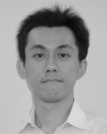
Author image of T. Meguro
Semiconductor Solutions Network Company, Sony Corporation, Tokyo, Japan
Tetsumasa Meguro received the B.S. and M.S. degrees in electrical engineering from the University of Tokyo, Tokyo, Japan, in 1993 and 1995, respectively.
In 1995, he joined Sony Corporation, Tokyo. He has been involved in the development of Video DSP. He is currently engaged in the development of low-power LSI design.
Tetsumasa Meguro received the B.S. and M.S. degrees in electrical engineering from the University of Tokyo, Tokyo, Japan, in 1993 and 1995, respectively.
In 1995, he joined Sony Corporation, Tokyo. He has been involved in the development of Video DSP. He is currently engaged in the development of low-power LSI design.View more
Author image of T. Seki
Semiconductor Solutions Network Company, Sony Corporation, Tokyo, Japan
Takahiro Seki received the B.S. and M.S. degrees in electrical engineering from the Tokyo University of Science, Japan, in 1990 and 1992, respectively.
In 1992, he joined Sony Corporation, Japan. He was engaged in research and development of CMOS digital and analog circuits, flash memory, and high-speed serial interface LSI. Since 1998, he has been engaged in research and development of low-power circuits and systems.
Takahiro Seki received the B.S. and M.S. degrees in electrical engineering from the Tokyo University of Science, Japan, in 1990 and 1992, respectively.
In 1992, he joined Sony Corporation, Japan. He was engaged in research and development of CMOS digital and analog circuits, flash memory, and high-speed serial interface LSI. Since 1998, he has been engaged in research and development of low-power circuits and systems.View more
Author image of T. Kondo
Semiconductor Solutions Network Company, Sony Corporation, Tokyo, Japan
Tetsuo Kondo received the B.S. degree in engineering from Shizuoka University, Shizuoka, Japan.
He joined Sony Corporation, Tokyo, Japan, in 1998, where he has been engaged in work on the dynamic voltage and frequency management technique and the low-power and reconfigurable processor.
Tetsuo Kondo received the B.S. degree in engineering from Shizuoka University, Shizuoka, Japan.
He joined Sony Corporation, Tokyo, Japan, in 1998, where he has been engaged in work on the dynamic voltage and frequency management technique and the low-power and reconfigurable processor.View more
Author image of A. Hashiguchi
Semiconductor Solutions Network Company, Sony Corporation, Tokyo, Japan
Akihiko Hashiguchi received the B.S. and M.S. degrees in energy conversion engineering from Kyusyu University, Japan, in 1998 and 1990, respectively.
In 1990, he joined Sony Corporation, Tokyo, Japan, where he designed DRAM. From 1993 to 1998, he was involved in the research of the Video DSP. From 1999, he researched the low power circuit and systems. Now, he is engaged in the development of sub-100-nm low-power LSI and th...Show More
Akihiko Hashiguchi received the B.S. and M.S. degrees in energy conversion engineering from Kyusyu University, Japan, in 1998 and 1990, respectively.
In 1990, he joined Sony Corporation, Tokyo, Japan, where he designed DRAM. From 1993 to 1998, he was involved in the research of the Video DSP. From 1999, he researched the low power circuit and systems. Now, he is engaged in the development of sub-100-nm low-power LSI and th...View more
Author image of H. Kawahara
Semiconductor Solutions Network Company, Sony Corporation, Tokyo, Japan
Hirokazu Kawahara received the B.S. degree in electrical engineering from the Tokyo University of Science, Japan, in 1984.
He joined Sony Corporation, Tokyo, where he has developed computer workstation systems. At present, he is engaged in development of low-power computer systems for mobile consumer products.
Hirokazu Kawahara received the B.S. degree in electrical engineering from the Tokyo University of Science, Japan, in 1984.
He joined Sony Corporation, Tokyo, where he has developed computer workstation systems. At present, he is engaged in development of low-power computer systems for mobile consumer products.View more
Author image of K. Kumano
Semiconductor Solutions Network Company, Sony Corporation, Tokyo, Japan
Kazuo Kumano received the B.S. degree in electrical engineering from the University of Hiroshima, Hiroshima, Japan.
In 1984, he joined Sony Corporation, Tokyo, Japan, where he has developed CMOS analog LSI circuits and system LSI circuits for cellular phones and PDAs since 1990.
Kazuo Kumano received the B.S. degree in electrical engineering from the University of Hiroshima, Hiroshima, Japan.
In 1984, he joined Sony Corporation, Tokyo, Japan, where he has developed CMOS analog LSI circuits and system LSI circuits for cellular phones and PDAs since 1990.View more
Author image of M. Shimura
Semiconductor Solutions Network Company, Sony Corporation, Tokyo, Japan
Masayuki Shimura received the B.S. degree in physics from Tsukuba University, Ibaraki, Japan.
In 1987, he joined Sony Corporation, Tokyo, Japan. He was involved in the development of image sensor and camera control generator LSI and signal processing LSI for CCD cameras. From 1997 to 2001, he was on loan to Sony LSI Design Inc., where he was engaged in the logic design of MOS LSI for camera and video applications and netwo...Show More
Masayuki Shimura received the B.S. degree in physics from Tsukuba University, Ibaraki, Japan.
In 1987, he joined Sony Corporation, Tokyo, Japan. He was involved in the development of image sensor and camera control generator LSI and signal processing LSI for CCD cameras. From 1997 to 2001, he was on loan to Sony LSI Design Inc., where he was engaged in the logic design of MOS LSI for camera and video applications and netwo...View more

I. Introduction

Dynamic voltage and/or frequency control schemes have been reported in [1]–[5]. Our approach offers both dynamic frequency control (DFC) and dynamic voltage control (DVC). Clock frequency is autonomously and dynamically controlled while supply voltage is adaptively controlled resulting in the leakage power compensation effect. This dynamic voltage and frequency management (DVFM) approach achieved 82% power reduction in a Personal Information Management (PIM) application.

Author image of M. Nakai
Semiconductor Solutions Network Company, Sony Corporation, Tokyo, Japan
Masakatsu Nakai received the B.S. and M.S. degrees in electronics engineering from Tokai University, Tokyo, Japan, in 1988 and 1990, respectively.
In 1990, he joined Sony Corporation, Tokyo, Japan, where he developed single chip microcontrollers, memories, and analog circuits. Since 1999, he has been engaged in research and development of low-power circuits and techniques for CMOS LSI.
Masakatsu Nakai received the B.S. and M.S. degrees in electronics engineering from Tokai University, Tokyo, Japan, in 1988 and 1990, respectively.
In 1990, he joined Sony Corporation, Tokyo, Japan, where he developed single chip microcontrollers, memories, and analog circuits. Since 1999, he has been engaged in research and development of low-power circuits and techniques for CMOS LSI.View more
Author image of S. Akui
Semiconductor Solutions Network Company, Sony Corporation, Tokyo, Japan
Satoshi Akui received the B.S. and M.S degrees from the Tokyo Institute of Technology, Tokyo, Japan, in 1986 and 1988, respectively.
He joined Sony Corporation, Tokyo, Japan, in 1988. Since then, he has been engaged in research and development of new design methodologies. Since 2000, he has been engaged in research and development of mobile application processors.
Satoshi Akui received the B.S. and M.S degrees from the Tokyo Institute of Technology, Tokyo, Japan, in 1986 and 1988, respectively.
He joined Sony Corporation, Tokyo, Japan, in 1988. Since then, he has been engaged in research and development of new design methodologies. Since 2000, he has been engaged in research and development of mobile application processors.View more
Author image of K. Seno
Semiconductor Solutions Network Company, Sony Corporation, Tokyo, Japan
Katsunori Seno received the B.S. and M.S. degrees in electrical engineering from Waseda University, Tokyo, Japan, in 1986 and 1988, respectively.
In 1988, he joined Sony Corporation, where he was engaged in the development of high-speed 4 Mb and 16 Mb CMOS SRAM and MPEG2 video DSP. From 1995 to 1997, he was a Visiting Researcher at the University of California, Berkeley, doing research in the field of low power. He rejoined Sony in 1998. He is currently heading development of low-power dynamic reconfigurable architecture and power management technology.
Mr. Seno is a Program Committee Member of the Symposium on VLSI Circuits.
Katsunori Seno received the B.S. and M.S. degrees in electrical engineering from Waseda University, Tokyo, Japan, in 1986 and 1988, respectively.
In 1988, he joined Sony Corporation, where he was engaged in the development of high-speed 4 Mb and 16 Mb CMOS SRAM and MPEG2 video DSP. From 1995 to 1997, he was a Visiting Researcher at the University of California, Berkeley, doing research in the field of low power. He rejoined Sony in 1998. He is currently heading development of low-power dynamic reconfigurable architecture and power management technology.
Mr. Seno is a Program Committee Member of the Symposium on VLSI Circuits.View more
Author image of T. Meguro
Semiconductor Solutions Network Company, Sony Corporation, Tokyo, Japan
Tetsumasa Meguro received the B.S. and M.S. degrees in electrical engineering from the University of Tokyo, Tokyo, Japan, in 1993 and 1995, respectively.
In 1995, he joined Sony Corporation, Tokyo. He has been involved in the development of Video DSP. He is currently engaged in the development of low-power LSI design.
Tetsumasa Meguro received the B.S. and M.S. degrees in electrical engineering from the University of Tokyo, Tokyo, Japan, in 1993 and 1995, respectively.
In 1995, he joined Sony Corporation, Tokyo. He has been involved in the development of Video DSP. He is currently engaged in the development of low-power LSI design.View more
Author image of T. Seki
Semiconductor Solutions Network Company, Sony Corporation, Tokyo, Japan
Takahiro Seki received the B.S. and M.S. degrees in electrical engineering from the Tokyo University of Science, Japan, in 1990 and 1992, respectively.
In 1992, he joined Sony Corporation, Japan. He was engaged in research and development of CMOS digital and analog circuits, flash memory, and high-speed serial interface LSI. Since 1998, he has been engaged in research and development of low-power circuits and systems.
Takahiro Seki received the B.S. and M.S. degrees in electrical engineering from the Tokyo University of Science, Japan, in 1990 and 1992, respectively.
In 1992, he joined Sony Corporation, Japan. He was engaged in research and development of CMOS digital and analog circuits, flash memory, and high-speed serial interface LSI. Since 1998, he has been engaged in research and development of low-power circuits and systems.View more
Author image of T. Kondo
Semiconductor Solutions Network Company, Sony Corporation, Tokyo, Japan
Tetsuo Kondo received the B.S. degree in engineering from Shizuoka University, Shizuoka, Japan.
He joined Sony Corporation, Tokyo, Japan, in 1998, where he has been engaged in work on the dynamic voltage and frequency management technique and the low-power and reconfigurable processor.
Tetsuo Kondo received the B.S. degree in engineering from Shizuoka University, Shizuoka, Japan.
He joined Sony Corporation, Tokyo, Japan, in 1998, where he has been engaged in work on the dynamic voltage and frequency management technique and the low-power and reconfigurable processor.View more
Author image of A. Hashiguchi
Semiconductor Solutions Network Company, Sony Corporation, Tokyo, Japan
Akihiko Hashiguchi received the B.S. and M.S. degrees in energy conversion engineering from Kyusyu University, Japan, in 1998 and 1990, respectively.
In 1990, he joined Sony Corporation, Tokyo, Japan, where he designed DRAM. From 1993 to 1998, he was involved in the research of the Video DSP. From 1999, he researched the low power circuit and systems. Now, he is engaged in the development of sub-100-nm low-power LSI and the embedded SRAM.
Mr. Hashiguchi has been a member of the IEICE Electrical Society Technical Committee on Integrated Circuits and Devices since 2001.
Akihiko Hashiguchi received the B.S. and M.S. degrees in energy conversion engineering from Kyusyu University, Japan, in 1998 and 1990, respectively.
In 1990, he joined Sony Corporation, Tokyo, Japan, where he designed DRAM. From 1993 to 1998, he was involved in the research of the Video DSP. From 1999, he researched the low power circuit and systems. Now, he is engaged in the development of sub-100-nm low-power LSI and the embedded SRAM.
Mr. Hashiguchi has been a member of the IEICE Electrical Society Technical Committee on Integrated Circuits and Devices since 2001.View more
Author image of H. Kawahara
Semiconductor Solutions Network Company, Sony Corporation, Tokyo, Japan
Hirokazu Kawahara received the B.S. degree in electrical engineering from the Tokyo University of Science, Japan, in 1984.
He joined Sony Corporation, Tokyo, where he has developed computer workstation systems. At present, he is engaged in development of low-power computer systems for mobile consumer products.
Hirokazu Kawahara received the B.S. degree in electrical engineering from the Tokyo University of Science, Japan, in 1984.
He joined Sony Corporation, Tokyo, where he has developed computer workstation systems. At present, he is engaged in development of low-power computer systems for mobile consumer products.View more
Author image of K. Kumano
Semiconductor Solutions Network Company, Sony Corporation, Tokyo, Japan
Kazuo Kumano received the B.S. degree in electrical engineering from the University of Hiroshima, Hiroshima, Japan.
In 1984, he joined Sony Corporation, Tokyo, Japan, where he has developed CMOS analog LSI circuits and system LSI circuits for cellular phones and PDAs since 1990.
Kazuo Kumano received the B.S. degree in electrical engineering from the University of Hiroshima, Hiroshima, Japan.
In 1984, he joined Sony Corporation, Tokyo, Japan, where he has developed CMOS analog LSI circuits and system LSI circuits for cellular phones and PDAs since 1990.View more
Author image of M. Shimura
Semiconductor Solutions Network Company, Sony Corporation, Tokyo, Japan
Masayuki Shimura received the B.S. degree in physics from Tsukuba University, Ibaraki, Japan.
In 1987, he joined Sony Corporation, Tokyo, Japan. He was involved in the development of image sensor and camera control generator LSI and signal processing LSI for CCD cameras. From 1997 to 2001, he was on loan to Sony LSI Design Inc., where he was engaged in the logic design of MOS LSI for camera and video applications and network I/F, DVD player, DTV, etc. In 2001, he rejoined Sony Corporation where he is currently General Manager of LSI Design Department for high-speed low-power processor SoC of mobile consumer products.
Masayuki Shimura received the B.S. degree in physics from Tsukuba University, Ibaraki, Japan.
In 1987, he joined Sony Corporation, Tokyo, Japan. He was involved in the development of image sensor and camera control generator LSI and signal processing LSI for CCD cameras. From 1997 to 2001, he was on loan to Sony LSI Design Inc., where he was engaged in the logic design of MOS LSI for camera and video applications and network I/F, DVD player, DTV, etc. In 2001, he rejoined Sony Corporation where he is currently General Manager of LSI Design Department for high-speed low-power processor SoC of mobile consumer products.View more

References

References is not available for this document.