Showing 1-25 of 6,876 resultsfor "Index Terms":Thin-film Technology
"Index Terms":Thin-film Technology
- Sort
Get notified when new research is published matching your search criteria.
Sort By
Results
Microstrip thin-film MCM-D technology on high-resistivity silicon with integrated through-substrate vias
G. Posada;G. Carchon;P. Soussan;N. Pham;B. Majeed;D. Sabuncouglu;W. Ruythooren;B. Nauwelaers;W. De Raedt
2007 European Microwave Integrated Circuit Conference
Year: 2007 | Conference Paper |
Cited by: Papers (10)
The integration of through-substrate vias on 100 mum thick high-resistivity silicon (HRSi) wafers within the thin-film multi-chip module technology (MCM-D) is demonstrated in this paper. High quality integrated lumped elements such as thin-film resistors, capacitors and inductors are demonstrated on a microstrip configuration within an MCM-D technology. Microstrip lines integrated on the thin HRSi...Show More
Microstrip thin-film MCM-D technology on high-resistivity silicon with integrated through-substrate vias
G. Posada;G. Carchon;P. Soussan;N. Pham;B. Majeed;D. Sabuncouglu;W. Ruythooren;B. Nauwelaers;W. De Raedt
The integration of through-substrate vias on 100 mum thick high-resistivity silicon (HRSi) wafers within the thin-film multi-chip module technology (MCM-D) is demonstrated in this paper. High quality integrated lumped elements such as thin-film resistors, capacitors and inductors are demonstrated on a microstrip configuration within an MCM-D technology. Microstrip lines integrated on the thin HRSi...Show More
Profiling innovation system for Solar Photovoltaics in China
2009 IEEE International Conference on Industrial Engineering and Engineering Management
Year: 2009 | Conference Paper |
China is rapidly emerging as an important player in the global photovoltaics market. By adopting a technology innovation systems framework of analysis, the paper identifies the technological and institutional actors and relations of the innovation systems for solar photovoltaics in China, and assesses the extent to which these are likely to encourage or constrain the technological development and ...Show More
Application of Dielectric, Ferroelectric and Piezoelectric Thin Film Devices in Mobile Communication and Medical Systems
M. Klee;D. Beelen;W. Keur;R. Kiewitt;B. Kumar;R. Mauczok;K. Reimann;Ch. Renders;A. Roest;F. Roozeboom;P. Steeneken;M. Tiggelman;F. Vanhelmont;O. Wunnicke;P. Lok;K. Neumann;J. Fraser;G. Schmitz
2006 15th ieee international symposium on the applications of ferroelectrics
Year: 2006 | Conference Paper |
Dielectric, ferroelectric and piezoelectric thin films are getting more and more attention for next generation mobile communication and medical systems. Thin film technologies based on dielectric, ferroelectric and piezoelectric thin films enable system-in-package (SiP) devices, resulting in optimal integration of various functions in one module with respect to high performance, small size and low...Show More
Application of Dielectric, Ferroelectric and Piezoelectric Thin Film Devices in Mobile Communication and Medical Systems
M. Klee;D. Beelen;W. Keur;R. Kiewitt;B. Kumar;R. Mauczok;K. Reimann;Ch. Renders;A. Roest;F. Roozeboom;P. Steeneken;M. Tiggelman;F. Vanhelmont;O. Wunnicke;P. Lok;K. Neumann;J. Fraser;G. Schmitz
Year: 2006 | Conference Paper |
Exploring spray technology for the fabrication of organic devices based on poly(3-hexylthiophene)
Alaa Abdellah;Daniela Baierl;Bernhard Fabel;Paolo Lugli;Giuseppe Scarpa
2009 9th IEEE Conference on Nanotechnology (IEEE-NANO)
Year: 2009 | Conference Paper |
Cited by: Papers (7)
In order to fully exploit the potential of polymer electronics, large-area/low-cost processing technologies are necessary. In this paper, we investigate the feasibility of air atomizing spray technology for large-area/low-cost fabrication of organic electronic and optoelectronic thin-film devices based on solution-processable polythiophene derivatives. For this purpose an airbrush coating system w...Show More
The Past, Present and Future of Space Photovoltaics
2006 IEEE 4th World Conference on Photovoltaic Energy Conference
Year: 2006 | Conference Paper |
Cited by: Patents (5)
This paper discusses the migration of crystalline space solar cell technology from silicon, to gallium arsenide then to the multiple junction devices in use today. Thin film technologies have migrated from the Cu2S/CdS and similar cells to the amorphous silicon multijunction devices to copper indium diselenide devices. Array technologies have moved from flat plate arrays with shingled cells to con...Show More
The novel multilayer thin-film substrate using BCB as a dielectric was suggested in the paper. 3-metals and 2-BCB layers were used in this technology for the evaluation of passive devices. The band pass filter for W-band application with unique circuit and structure was designed and implemented. The implemented filter has an insertion loss below 1.5 dB, and return loss over 20 dB in the passband o...Show More
A V-Band Beam-Steering Antenna on a Thin-Film Substrate With a Flip-Chip Interconnection
Sanghyo Lee;Sangsub Song;Youngmin Kim;Jangsoo Lee;Chang-Yul Cheon;Kwang-Seok Seo;Youngwoo Kwon
We propose a planar V-band beam-steering antenna based on a millimeter-wave (mm-wave) system-on-package technology using advanced thin-film technology on a silicon mother board. The thin-film substrate has the capability of integrated passive elements and flip-chip interconnection. Space-consuming components such as a microstrip Rotman lens and patch antennas are implemented on a low-loss, low-cos...Show More
Features of thin film CVD processes used in IC device technology
2009 International Conference and Seminar on Micro/Nanotechnologies and Electron Devices
Year: 2009 | Conference Paper |
Basic film step coverage and gap-fill data has been consolidated and compared with the observed thin film CVD kinetics trends. Based on some assumptions regarding reaction kinetics, obtained correlations are believed to be applicable for an optimization of ultra small gap filling in deep submicron integrated circuit technology.Show More
Trends of Research and Dissemination for PV Systems in Korea
2006 IEEE 4th World Conference on Photovoltaic Energy Conference
Year: 2006 | Conference Paper |
Cited by: Papers (1)
Korea strategically selected PV as one of the major renewable energy technologies and thus rapidly expanded PV program both for R&D and dissemination since 2004. The Korean Government established Korean Photovoltaic Development Organization in 2004 and commissioned it with planning and managing R&D program. The R&D program focuses on manufacturing technologies necessary for reducing the system cos...Show More
Green technologies for building material business
Lawrence Carter;Woraruthai Choothian;Nuttawut Intrarode;Pattravadee Ploykitikoon
PICMET '09 - 2009 Portland International Conference on Management of Engineering & Technology
Year: 2009 | Conference Paper |
Technology assessment is one aspect of the technology acquisition process. This process provides a framework that helps companies thoroughly understand their necessities and capabilities in order to select appropriate emerging technologies from the right sources for the companies at the right time. With rapid changes in technology and boundless customer needs in our globalization era, these implic...Show More
Thin film devices
2009 Device Research Conference
Year: 2009 | Conference Paper |
First Page of the Article
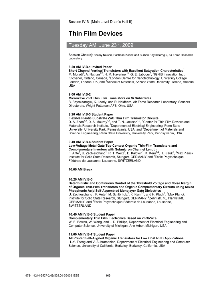 Show More
An all-organic technology platform for electronic devices manufacturing
M. La Rosa;G. Coppola;P. Dardano;N. Malagnino;A. Marcellino;D. Nicolosi;L. Occhipinti;F. Porro;I. Rendina;G. Sicurella;R. Vecchione;E. Umana
In this work a complete and dedicated technology platform for all-organic electronic applications with micron and sub-micron feature-size is proposed. Both the organic technology and the design tools have been developed by considering organic materials to be deposited by solution techniques. The complete process flow has been defined in order to realize multilayered functional structures as all-or...Show More
Materials on the International Space Station Experiment-5, Forward Technology Solar Cell Experiment: First On-Orbit Data
R. J. Walters;D. M. Garner;S. N. Lam;J. A. Vasquez;W. R. Braun;R. E. Ruth;J. H. Warner;J. R. Lorentzen;S. R. Messenger;CDR R. Bruninga;P. P. Jenkins;J. M. Flatico;D. M. Wilt;M. F. Piszczor;L. C. Greer;M. J. Krasowski
2006 IEEE 4th World Conference on Photovoltaic Energy Conference
Year: 2006 | Conference Paper |
Cited by: Papers (4)
First on-orbit data from the forward technology solar cell experiment (FTSCE) are presented. FTSCE is housed within the 5th Materials on the International Space Station Experiment (MISSE-5), and currently resides on the exterior of the ISS. A range of solar cell technologies are included in the experiment including triple junction (3J) InGaP/GaAs/Ge solar cells from several vendors, thin film amo...Show More
Materials on the International Space Station Experiment-5, Forward Technology Solar Cell Experiment: First On-Orbit Data
R. J. Walters;D. M. Garner;S. N. Lam;J. A. Vasquez;W. R. Braun;R. E. Ruth;J. H. Warner;J. R. Lorentzen;S. R. Messenger;CDR R. Bruninga;P. P. Jenkins;J. M. Flatico;D. M. Wilt;M. F. Piszczor;L. C. Greer;M. J. Krasowski
San Jose State University is initiating a new undergraduate BS degree program in Microelectronics Process Engineering. The program is being developed by a team of faculty in chemical and materials engineering. The program is designed to provide the broad engineering fundamentals expected of any undergraduate engineering degree, as well as specific science, process design and process engineering of...Show More
Analysis of Fabrication Techniques for Thin Film Schottky Diode for 5G and Beyond
2024 International Conference on Electrical Electronics and Computing Technologies (ICEECT)
Year: 2024 | Conference Paper |
Thin film technology is made of material ranging from nanometers to micrometer in thickness. Thin film technology was developed to cater the needs of the IC industry. High demand for thin films compatible with high speed devices has introduced us to updated fabrication technologies. Knowledge of properties of thin nano-films and electronic devices such as diodes, transistors, capacitors can be sha...Show More
Development and Realization of a Doubleface Populated Multichip Module in Thin Film Technology for High Frequency Application
Proceedings of the International Conference on Multichip Modules
Year: 1994 | Conference Paper |
A doubleface populated transmit/receive (TR) multichip module for radar applications has been implemented with multilayer integration technology. The multilayer is designed and fabricated in thin film technology on A1203 ceramic substrates and offers a high order of complexity for high frequency (hf/rf) circuits up to 20 GHz. 100 /spl mu/m striplines with integrated thin film resistors in combinat...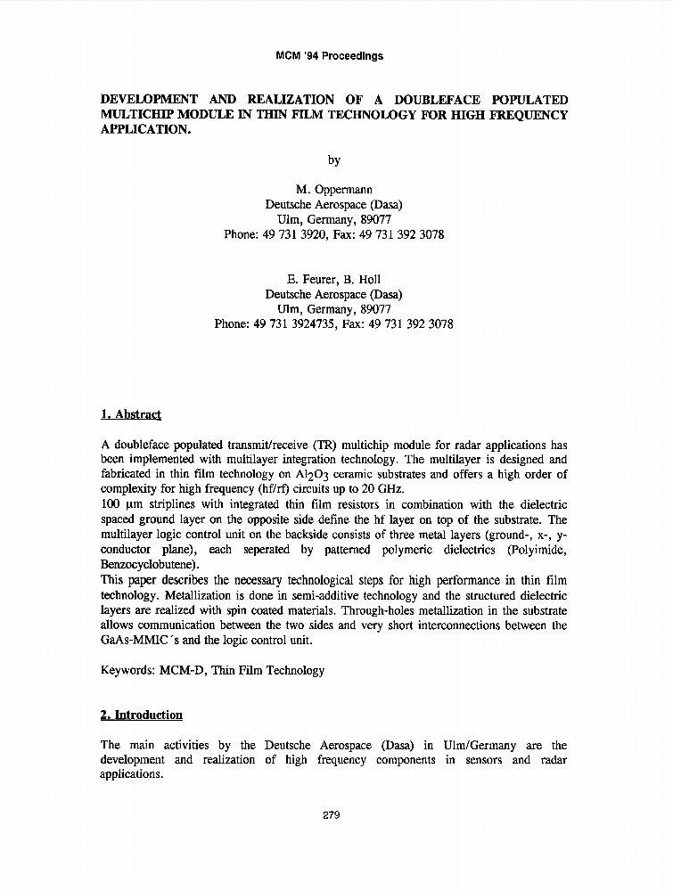 Show More
First Page of the Article
Show MorePrototype development - flexible Cu(In,Ga)Se/sub 2/ thin film solar cells for space applications
A. Neisser;C.A. Kaufmann;R. Klenk;R. Scheer;M.A. Kroon;G. Oomen;H.-W. Schock
Conference Record of the Thirty-first IEEE Photovoltaic Specialists Conference, 2005.
Year: 2005 | Conference Paper |
Cited by: Papers (2)
Flexible thin film technologies find increased attention with device efficiencies approaching values comparable to rigid substrates. In particular the high power to weight ratio plus the superior radiation hardness of flexible thin film solar cells make them an attractive alternative to current technologies for space power generation. This contribution reports on latest advances in the development...Show More
Advanced packaging of integrated passive devices for RF applications
Proceedings RAWCON 98. 1998 IEEE Radio and Wireless Conference (Cat. No.98EX194)
Year: 1998 | Conference Paper |
Modern RF and wireless systems, in particular the portable and handheld consumer devices, are placing huge demands on component and assembly technologies. The integration of many different functions into one unit means that the component count has become very large. Since passive components form the majority of the devices mounted on the circuit board, there is considerable incentive to identify w...Show More
Side-by-Side Comparison of Single- and Dual-Active Layer Oxide TFTs: Experiment and TCAD Simulation
Kevin A. Stewart;Vasily Gouliouk;John M. McGlone;John F. Wager
Single-active layer (SAL) and dual-active layer (DAL) oxide thin-film transistors (TFTs) are fabricated using the same process conditions and compared side by side. The SAL channel consists of amorphous In-Ga-Zn-O (a-IGZO), and the DAL of ultrathin In-Sn-O and a-IGZO. The DAL TFT exhibits strongly improved performance compared to the SAL TFT such as higher mobility of 31 cm2·V-1·s-1, smaller subth...Show More
Developing a novel patent map to explore R&D directions and technical gaps for thin-film photovoltaic industry
2009 IEEE International Conference on Industrial Engineering and Engineering Management
Year: 2009 | Conference Paper |
Cited by: Papers (4)
This paper addresses a novel technical patent map to effectively mining the patent information among assignee, patent classification, and filing date on thin-film photovoltaic. The proposed technical patent map provides an overall view of technological advancement that allows researchers to monitor competitor deployments, mine the techniques gap, and forecast technology trends. There are 164 paten...Show More
Thin-film photovoltaic radiation testing and modeling for a MEO orbit
J.E. Granata;T.D. Sahlstrom;P. Hausgen;S.R. Messenger;R.J. Walters;J.R. Lorentzen
Conference Record of the Thirty-first IEEE Photovoltaic Specialists Conference, 2005.
Year: 2005 | Conference Paper |
Cited by: Papers (10)
A radiation test plan for thin-film photovoltaic technologies focused on a MEO flight experiment is outlined. The radiation response of thin film, triple junction amorphous Si solar cells, with and without a space coating, is presented. The degradation of the photovoltaic output under 2 MeV proton irradiation is measured and analyzed. Irradiations performed both at room temperature, in the dark, a...Show More
Organic thin film electronics
IEEE InternationalElectron Devices Meeting, 2005. IEDM Technical Digest.
Year: 2005 | Conference Paper |
Cited by: Papers (1)
The technological landscape appears ripe for an explosion of organic electronic applications. Devices with performance exceeding a-Si:H thin film transistors have been demonstrated and applications that use the particular strengths of organic devices are beginning to emerge. All-organic displays have been demonstrated and solution processed materials with device performance similar to vapor deposi...Show More
Complementary thin film electronics based on ZnO/ZnTe
2009 Device Research Conference
Year: 2009 | Conference Paper |
Thin film transistors for large-area and/or flexible electronics desire materials with the maximum carrier mobility while maintaining a reasonable deposition temperature. Semiconducting oxides including polycrystalline ZnO and amorphous IGZO have emerged as important candidates for thin film transistors due to their relatively high carrier mobility (~10cm2/Vs) in comparison to amorphous silicon an...Show More
Status And Future Prospects For Thin Film Amorphous Silicon And Polycrystalline Solar Cells
Electro International, 1991
Year: 1991 | Conference Paper |
Thin-film photovoltaics are emerging as a low cost alternative to the present crystalline silicon solar cell technology. The present status and future prospects of three thin-film technologies based on Amorphous Silicon, Copper-Indium-Selenide and Cadmium Telluride are reviewed.Show More
IEEE Account
Purchase Details
Profile Information
Need Help?
- US & Canada: +1 800 678 4333
- Worldwide: +1 732 981 0060
- Contact & Support
- About IEEE Xplore
- Contact Us
- Help
- Accessibility
- Terms of Use
- Nondiscrimination Policy
- Sitemap
- Privacy & Opting Out of Cookies
A not-for-profit organization, IEEE is the world's largest technical professional organization dedicated to advancing technology for the benefit of humanity.
© Copyright 2025 IEEE - All rights reserved. Use of this web site signifies your agreement to the terms and conditions.